Extreme Low Power/Energy System Design
Power consumption has become a zeroth order design constraint in digital
design today, for both tethered and mobile electronics.
My group has made several contributions to this area, by demonstrating
practical means to develop extreme low power circuit designs.
The use of sub-threshold circuits enables significant power savings
(100X-500X for a 90nm fabrication process) with a modest reduction in
operating speed. However, sub-threshold circuits exhibit a delay
variation of between 100X and 1000X when factors like temperature,
processing and power supply variations are accounted for. As a result,
they have not been used in practical IC products so far.
My group has solved the sub-threshold delay variation problem by
using an adaptive bulk biasing (ABB) scheme. Raising or lowering the bulk
node voltage can speed up or slow down a VLSI circuit. ABB involves
dynamically adjusting the bulk node voltage in a closed-loop fashion, to
lock the circuit delay to a user-specified value. Using NSF and LLNL
funding, my group fabricated a 250nm ABB based sub-threshold circuit with
complete success, demonstrating a 20X power improvement. A conservative
improvement of 100X is estimated if we had used a 90nm process. This work was
initially part of an interdisciplinary project whose goal was to develop
extreme low power, insect-borne electronics.
In addition, we have developed techniques to find the supply voltage that
minimizes the energy of a sub-threshold design, as well as asynchronous
micropipelining approaches to recover the delay penalty (by 7X) of
sub-threshold designs. Other work in this area includes low power/energy
bus design for data transfers, as well as low power SRAM memory design.
Publications, patents and artefacts:
- "A Variation-tolerant
Sub-threshold Design Approach", Jayakumar,
Khatri. Design Automation Conference (DAC), 2005 Anaheim, CA , June 13-17,
pp. 716-719. This paper first presented our ABB based delay variation
canceling methodology, and achieves a 2 order of magnitude reduction in
delay variation compared to the case where no delay compensation is done. Presentation slides.
- "Minimum Energy Near-threshold Network of PLA
based Design", Jayakumar,
Khatri. International Conference on Computer Design (ICCD) 2005, Oct 2-5,
San Jose, CA, pp. 399-404. This paper reports our findings on techniques to
find the energy-minimizing supply voltage for sub-threshold designs. The
paper shows that for energy minimality, the supply voltage is slightly
above the threshold voltage, and depends on logic depth.
- "A PLA based Asynchronous Micropipelining Approach for Subthreshold
Circuit Design", Jayakumar, Garg, Gamache, Khatri. ACM/IEEE Design
Automation Conference (DAC), July 24-28 2006, pp. 419-424. This paper
describes our work on reclaiming the speed penalty of sub-threshold designs by
micropipelining. This paper achieves a 7X speedup over a non-micropipelined
approach, with a 47%. Presentation slides.
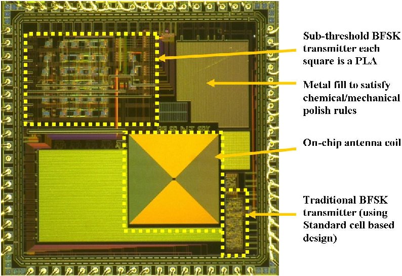
- "Design and Implementation of a Sub-threshold BFSK
Transmitter", Paul,
Garg, Khatri, Vaidya. International Symposium on Quality Electronic Design
(ISQED) San Jose, CA. Mar 16-18 2009. This paper describes the design
methodology used in designing our sub-threshold transmitter IC, along with results
obtained from silicon. The chip achieves a 20X power reduction compared to
a super-threshold implementation of the same circuit on the same die (in a
250nm process) Presentation slides.
- "RF Receiver and Transmitter for Insect Mounted
Sensor Platform", Duperre,
Burgett, Garg, Khatri. IEEE Midwest Symposium on Circuits and Systems (MWSCAS) 2009, Cancun, Mexico. August 2-5, 2009. This
paper describes our work in designing the transmitter (which uses our
sub-threshold transmitter IC) and receiver systems for the sponsored
project.
- Invited Paper"Extreme Low Power Computing using Sub-threshold
Circuits", Segundo Magno Congreso Interancional del CIC 2007, Mexico
City, Mexico, November 6-8, 2007. This paper presented a summary of our
work in sub-threshold system design.
- "Encoding Serial Data for Graphical
EDP/Energy Minimization", Ekambavananan, Garg, Khatri. Accepted for
publication at the Journal of Low Power Electronics (JOLPE), Vol. 5,
No. 2, August 2009. This paper reports on methods for reducing energy
and the energy-delay-product for serial data transmission, using a
3-codebook algorithm.
- "Selective Forward Body Bias for High Speed and Low Power SRAMs",
Bollapalli, Garg, Gulati, Khatri. Accepted for publication at the Journal
of Low Power Electronics (JOLPE), Vol. 5, No. 2, August 2009. In this
paper, we design a SRAM with devices that are nominally reverse biased, and
are forward biased just in time for an access. We show that not only does
the modified SRAM consume less power, but it is also faster.
- "Energy Efficient and High Speed On-Chip
Ternary Bus", Duan, Khatri. Design
Automation, and Test in Europe (DATE) Conference 2008, 10-14 March, Munich,
Germany, pp. 515-518. In this paper, we present a half-swing, encoded
ternary bus design. Although the bus drives 3 voltages, they are
encoded to 2 logic values, yielding a faster, lower power bus design.
- "Minimizing and Exploiting Leakage in VLSI Design", Jayakumar, Paul,
Garg, Khatri. Monograph published by Springer Publishers. 1st edition,
2010. 214p. ISBN 978-1-4419-0949-7. This monograph describes our work in
sub-threshold design, as well as leakage minimization.
- U.S. Patent 7880505: "Low Power Reconfigurable Circuits with Delay
Compensation", Khatri, Vaidya, Griffin, Jayakumar. Issued Feb 2011. This
patent on extreme low power reconfigurable circuit technology was filed
through Texas A&M.