For my final project in CSCE 450 I decided to create a circuit visualizer. An overview of the project can be viewed in this video.
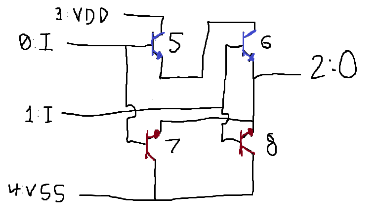
This visualizer was designed to act on an input file generated by another program. In the project proposal, the final product was described to have several processing steps to create a clean visualization. The first step was the layout algorithm for placing nodes, or transistors, in a way that has max symmetries. The next step was to draw the wires that connect the nodes in an orthographic manner. An example of the kind of image I wanted to create is below.
I was only able to get the first part kind of done. After reading in the file and getting a framebuffer drawing to the screen, I implemented a PDB algorithm to try to layout the nodes. This turned out to be much more difficult than expected to get a good result, and I was unable to complete any of the other steps. However, I was able to visualize the pdb steps and make a halfway decent visualization of that.

I'm not very happy with how this project turned out, and I aim to improve it in the future.