Research
-
Compressed Sensing
Compressed Sensing

A Sub-Nyquist Rate Compressive Sensing Data Acquisition Front-End
IEEE Journal on Emerging and Selected Topics in Circuits and Systems, Vol. 2, No. 3, pp. 482-492, Sept. 2012

Digital-Assisted Asynchronous Compressive Sensing Front-End
IEEE Journal on Emerging and Selected Topics in Circuits and Systems, Vol. 2, No. 3, pp. 542-551, Sept. 2012

The impact of ADC nonlinearity in a mixed-signal compressive sensing system for frequency-domain sparse signals
Physical Communication, 17 November 2011
-
Analog to Digital Conversion
Analog to Digital Conversion

Sensitivity Analysis of Continuous-Time Delta-Sigma ADCs to Out-of-Band Blockers in Future SAW-Less Multi-Standard Wireless Receivers
IEEE Transactions on Circuits and Systems I, Vol. 59, No. 9, pp. 1894-1905, Sept. 2012.

Feed-Forward Spectral Shaping Technique for Clock-Jitter Induced Errors in Digital-to-Analog Converters
IET Electronics Letters, Vol 47, Issue 3, pp. 826-828, Feb. 2011.

Sensitivity of single-bit continuous-time analogue-to-digital converters to out-of-band blockers
IET Electronics Letters, Vol. 46, No. 12, pp. 826–828, June 2010.
-
Multi-Channel Transceivers
Multi-Channel Transceivers

Clock-Jitter-Tolerant Wideband Receivers: An Optimized Multichannel Filter-Bank Approach
Circuits and Systems I: Regular Papers, IEEE. Feb. 2011

Least Mean Squared Background Calibration For OFDM Multi Channel Receivers
Journal of Circuits, Systems, and Computers, Volume 21, Issue 01, February 2012.

Analytical Framework and Bandwidth Optimization of OFDM Low-Order Multi-Channel Filter-Bank Receivers for Achieving Sampling Clock-Jitter-Robustness
IET Circuits Devices Syst. September 2011.
-
Medical Sensing
Medical Sensing

Compressed Digital Beamformer With Asynchronous Sampling For Ultrasound Imaging
A Compressed Digital Beamformer (CDB) framework for the design of an ultrasound imaging system with a large transducer array.

Digital-Assisted Asynchronous Compressive Sensing for Ultra-low Power ECG Wireless Recording
State-of-the-art wireless medical sensing and monitoring systems have imposed very high demands on accuracy, low power and portable solutions.
-
Analog Signal Processing
Analog Signal Processing

A 2.8 mW Sub-2 dB Noise Figure Inductorless Wideband CMOS LNA Employing Multiple Feedback
IEEE Transactions on Microwave Theory and Techniques, Vol. 59, pp. 3154 - 3161, Issue 12, Dec. 2011.

Reduced Area Discrete-Time Down-Sampling Filter Embedded with Windowed Integration Samplers
IET Electronics Letters, Vol. 46, Issue 12, pp. 828–830, June 2010.

Wideband Common-Gate CMOS LNA Employing Dual Negative Feedback with Simultaneous Noise, Gain, and Bandwidth Optimization
IEEE Transactions On Microwave Theory And Techniques, Vol. 58, No. 9, pp. 2340-2351, Sept. 2010
Compressed Sensing
A Sub-Nyquist Rate Compressive Sensing Data Acquisition Front-End
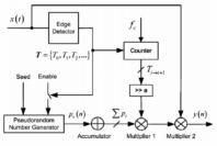
This paper presents a sub-Nyquist rate data acquisition front-end based on compressive sensing theory. The front-end randomizes a sparse input signal by mixing it with pseudo-random number sequences, followed by analog-to-digital converter sampling at sub-Nyquist rate. The signal is then reconstructed using an L1-based optimization algorithm that exploits the signal sparsity to reconstruct the signal with high fidelity. The reconstruction is based on a priori signal model information, such as a multi-tone frequency-sparse model which matches the input signal frequency support. Wideband multi-tone test signals with 4% sparsity in 5~500 MHz band were used to experimentally verify the front-end performance. Single-tone and multi-tone tests show maximum signal to noise and distortion ratios of 40 dB and 30 dB, respectively, with an equivalent sampling rate of 1 GS/s. The analog front-end was fabricated in a 90 nm complementary metal–oxide–semiconductor process and consumes 55 mW. The front-end core occupies 0.93 mm.
Digital-Assisted Asynchronous Compressive Sensing Front-End
Compressive sensing (CS) is a promising technique that enables sub-Nyquist sampling, while still guaranteeing the reliable signal recovery. However, existing mixed-signal CS frontend implementation schemes often suffer from high power consumption and nonlinearity. This paper presents a digital-assisted asynchronous compressive sensing (DACS) front-end which offers lower power and higher reconstruction performance relative to the conventional CS-based approaches. The front-end architecture leverages a continuous-time ternary encoding scheme which modulates amplitude variation to ternary timing information. Power is optimized by employing digital-assisted modules in the front-end circuit and a part-time operation strategy for high-power modules. An -member Group-based Total Variation ( -GTV) algorithm is proposed for the sparse reconstruction of piecewise-constant signals. By including both the inter-group and intra-group total variation, the -GTV scheme outperforms the conventional TV-based methods in terms of faster convergence rate and better sparse reconstruction performance. Analyses and simulations with a typical ECG recording system confirm that the proposed DACS front-end outperforms a conventional CS-based front-end using a random demodulator in terms of lower power consumption, higher recovery performance, and more system flexibility.
The impact of ADC nonlinearity in a mixed-signal compressive sensing system for frequency-domain sparse signals
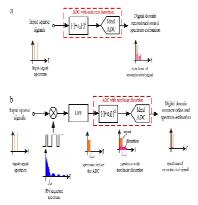
Compressive sensing (CS) holds new promises for the digitization of wideband frequency-domain sparse signals at sub-Nyquist rate sampling without compromising the reconstruction quality. In this paper, the impact of ADC nonlinearity in a CS receiver for frequency-domain sparse signals is investigated. In a mixed-signal CS system, signals are randomized before sampling. The signal spectrum at each building block in the mixedsignal CS system is analyzed and compared to a conventional Nyquist-rate sampling system. It is shown that the signal randomization in a mixed-signal CS system is able to spread the spurious energy due to ADC nonlinearity along the signal bandwidth, rather than the concentration of harmonic distortion on a few frequencies as it is the case for a conventional ADC. As a result, this paper shows that a significant ADC SFDR (Spurious Free Dynamic Range) improvement is achieved in a CS receiver when processing sparse signals.Simulation results are reported which are in good agreement with the qualitative analysis.
Analog to Digital Conversion
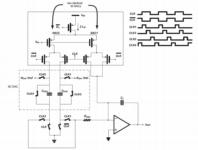
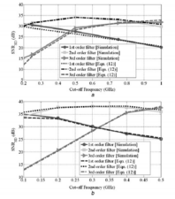
Sensitivity Analysis of Continuous-Time ADCs to Out-of-Band Blockers in Future SAW-Less Multi-Standard Wireless Receivers
The increasing demand for integrating multiple wireless services in one multi-standard handset, exemplified by the software- defined radio (SDR) model, calls for digitizing wireless receivers in a quest for flexibility. Radio-frequency (RF) front-end and analog baseband filters need to be exchanged for digital processing at the expense of a highly challenging analog-to-digital converter (ADC) specifications. In this paper, the sensitivities of continuous- time (CT) delta-sigma ADCs, which are candidate architectures for multi-standard receivers and SDRs, to out-ofband (OOB) blockers at the ADC input are investigated. This analysis addresses the problems and performance limitations that can result from large OOB blockers appearing at the input of CT modulators in a digitized multi-standard receiver. Analysis and discussions given in different sections of the paper are verified by CT system-level simulations.
Feedforward spectral shaping technique for clock-jitter induced errors in digital-to-analogue converters
A simple feedforward spectral shaping technique for the pulsewidth jitter induced errors in digital-to-analogue converters (DACs) is presented. The proposed technique features a feedforward combination of the conventional rectangular-pulse switched-current DAC and a discrete-time switched-capacitor DAC to achieve spectral shaping for the jitter induced error. The benefit of this hybrid DAC solution using error specral shaping is illustrated in the context of feedback DACs used in continuous-time DS modulators. Simulation results show that the jitter tolerance of the proposed DAC solution is equivalent to that of the commonly used jitter-tolerant exponentially-decaying waveform switched-capacitor-resistor DAC structure, but at much more relaxed slew-rate requirement on the op-amp used in the DAC load circuit, which translates into significant power savings.
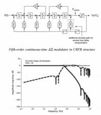
Sensitivity of single-bit continuous-time DS analogue-to-digital converters to out-of-band blockers
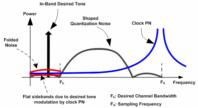
The sensitivity of single-bit continuous-time (CT) DS analogue-todigital converters to out-of-band (OOB) blockers received in companion with desired signals is investigated. In essence, the residual interferer signal appearing at the output of the CT loop filter can flip the single-bit quantiser decision near the zero crossings of the loop filter output signal. An intuitive analysis of this effect on the performance of single-bit DS modulators in the presence of OOB interferers is provided. System level simulations for a single-bit fifth-order CT DS modulator at an oversampling ratio of 40 have been carried out. A reduction in the achievable signal-to-noise-plus-distortion ratio, that can be as large as 10 dB when applying a 0 dBFS OOB blocker tone along with a weak 275 dBFS desired tone, has been observed. The simulation results show good agreement with the adopted theoretical discussion.
Multi-Channel Transceivers
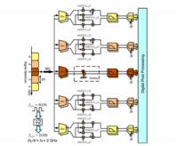
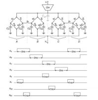
Clock-Jitter-Tolerant Wideband Receivers: An Optimized Multichannel Filter-Bank Approach
Jitter is one of the most fundamental obstacles in realizing future generations of wideband receivers. Stringent jitter specifications in the sampling clocks of high-performance single-channel and multichannel time-interleaved analog-to-digital converters severely limit the evolution of baseband receivers. This paper presents an analytical framework for the design of clock-jitter-tolerant low-order multichannel filter-bank receivers, with techniques to dramatically lower the sampling-clock-jitter specifications. Although it is well understood that high-order frequency-channelized receivers provide higher tolerance to sampling jitter, this paper shows that low-order bandwidth-optimized multichannel receivers can achieve similar sampling-jitter tolerance. Additionally, this paper presents design tradeoffs and specifications of an example multichannel receiver that can process a 5-GHz baseband signal with 40 dB of signal-to-noise-ratio using sampling clocks that can tolerate up to 5 psrms clock jitter. In comparison, existing architectures based on time-interleaving require 0.5 psrms clock jitter for the given specifications. This extreme jitter tolerance allows for relaxed design of clocking systems, which averts a major roadblock in future wideband-communication-receiver development and provides the potential
Least Mean Squared Background Calibration for OFDM Multichannel Receivers
This paper presents a data estimation scheme for wide band multichannel charge sampling filter bank receivers together with a complete system calibration algorithm based on the least mean squared (LMS) algorithm. A unified model has been defined for the receiver containing all first order mismatches, offsets, imperfections, and the LMS algorithm is employed to track these errors. The performance of this technique under noisy channel conditions has been verified. Moreover, a detailed complexity analysis of the calibration algorithm is provided which shows that sinc filter banks have much lower complexity than traditional continuoustime filter banks.
Analytical framework and bandwidth optimisation of orthogonal frequency division multiplexing low-order multi-channel filter-bank receivers for achieving sampling clock-jitter robustness
Stringent jitter specifications in the sampling clocks severely limit the evolution of future generations of wideband high-performance receivers. For instance, it is shown that a conventional single-channel receiver requires 1.5 ps of jitter standard deviation to achieve 34 dB signal-to-noise ratio (SNR) when sampling a 10 GHz orthogonal frequency division multiplexing (OFDM) signal. This study presents an analytical framework for the design of jitter-tolerant multi-channel filterbank OFDM receivers. Additionally, the study presents an optimisation method for the filter-bank bandwidth that is able to reduce the filter-bank order saving power and area and achieving optimal signal quality. Simulations that confirm the analytical result show that 34 and 38 dB SNR are achieved with 5-channel and 10-channel receivers, respectively, when using second-order bandwidth-optimised filter-bank that samples a 10 GHz OFDM signal tolerating 6 ps of jitter.
Medical Sensing
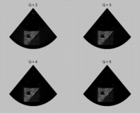
Compressed Digital Beamformer With Asynchronous Sampling For Ultrasound Imaging
The traditional Nyquist sampling architecture does not provide a feasible solution in a large multi-channel ultrasound imaging system. The main issues are the huge data volume after the analog-to-digital interface, high power consumption, and circuit complexity at both the front-end and mid-end. This paper presents a Compressed Digital Beamformer (CDB) framework for the design of an ultrasound imaging system with a large transducer array ( ≥ 1024) operating at a moderate carrier frequency ( ≥ 5 MHz). Simulations demonstrate that the proposed CDB framework achieves a Compression Ratio (CR) of 0.1 and Mean Square Error (MSE) of -27.7 dB with 4 quantization bits.
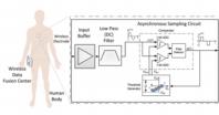
Digital-Assisted Asynchronous Compressive Sensing for Ultra-low Power ECG Wireless Recording
State-of-the-art wireless medical sensing and monitoring systems have imposed very high demands on accuracy, low power and portable form factor. Portable medical systems enjoy the non-intrusive form factors for use in free living conditions, but meanwhile, they are challenged by the limited power and storage resources for continuous monitoring. As a result, power consumption in the order of 1nW/bit in the wireless link is specified by IEEE 802.15 TG6. Systems which utilize traditional analog-to-digital converters (ADC) must have a sampling rate that is at least twice the signal’s bandwidth according to the famous Shannon/Nyquist sampling theorem. However, even for designs in advanced technology nodes, high sampling rates usually lead to excessive power consumption and become one of major challenges for portable battery-powered systems. Although advanced digital signal processing (DSP) algorithms such as compression algorithms (i.e., Arithmetic coding and Lempel-Ziv coding) can reduce overall power consumption by decreasing the data rate in energy- demanding radio links, most of these techniques require Nyquist sampling at the input. A natural question arises, if the target signal has some special characteristics, such as sparse, compressible, piecewise-constant, etc., is it possible to realize sub-Nyquist sampling without compromising the recovery performance?
Analog Signal Procesing
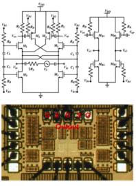
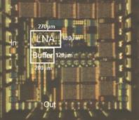
A 2.8-mW Sub-2-dB Noise-Figure Inductorless Wideband CMOS LNA Employing Multiple Feedback
A wideband low-noise amplifier (LNA), which is a key block in the design of broadband receivers for multiband wireless communication standards, is presented in this paper. The LNA is a fully differential common-gate structure. It uses multiple feedback paths, which add degrees of freedom in the choice of the LNA transconductance to reduce the noise figure (NF) and increase the amplification. The proposed LNA avoids the use of bulky inductors that leads to area and cost saving. A prototype is implemented in IBM 90-nm CMOS technology. It covers the frequency range of 100 MHz to 1.77 GHz. The core consumes 2.8 mW from a 2-V supply occupying an area of 0.03 mm2. Measurements show a gain of 23 dB with a 3-dB bandwidth of 1.76 GHz. The minimum NF is 1.85 dB, while the average NF is 2 dB across the whole band. The LNA achieves a return loss greater than 10 dB across the entire band and a third-order input intercept point IIP3 of 2.85 dBm at the maximum gain frequency.
Reduced area discrete-time down-sampling filter embedded with windowed integration samplers
A technique to implement a discrete-time (DT) sinc3 2 filter for windowed integration samplers is proposed. The topology reduces the idle time of the integration capacitors at the expense of a small complexity overhead in the clock generation, thereby saving 33% of the die area compared to the currently existing topology. Circuit level simulations in 45 nm CMOS technlogy shows good agreement with the predicted behaviour obtained from the analaysis.
Wideband Common-Gate CMOS LNA Employing Dual Negative Feedback With Simultaneous Noise, Gain, and Bandwidth Optimization
This paper presents a wideband common-gate (CG) LNA architecture that overcomes the fundamental tradeoff between power and noise match without compromising its stability. The proposed architecture can achieve the minimum noise figure (NF) over the previously reported feedback amplifiers in a CG configuration. The proposed architecture achieves broadband impedance matching, low noise, large gain, enhanced linearity, and wide bandwidth concurrently by employing an efficient and reliable dual negative-feedback. An amplifier prototype was realized in 0.18- m CMOS, operates from 1.05 to 3.05 GHz, and dissipates 12.6 mW from 1.8-V supply while occupying a 0.073-mm2 active area. The LNA provides 16.9-dB maximum voltage gain, 2.57-dB minimum NF, better than 10-dB input matching, and 0.7-dBm minimum IIP3 across the entire bandwidth.